
.jpg?x-oss-process=image/resize,w_100/quality,q_100)
.jpg?x-oss-process=image/resize,w_100/quality,q_100)
.jpg?x-oss-process=image/resize,w_100/quality,q_100)
.jpg?x-oss-process=image/resize,w_100/quality,q_100)

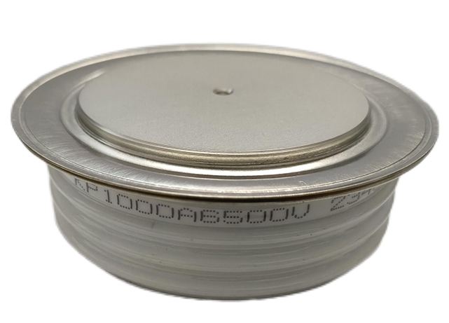
YZPST-KP1000A6500V
P/N:YZPST-KP1000A/6500V
ВЫСОКОМОЩНЫЙ ТИРИСТОР ДЛЯ ПРИМЕНЕНИЯ В СИСТЕМАХ ФАЗОВОГО УПРАВЛЕНИЯ
Особенности:
. Вся диффузионная структура
. Конфигурация с центральным усилением ворот
. Гарантированное максимальное время выключения
. Высокая способность к dV/dt
. Давлением собранный прибор


P/N:YZPST-KP1000A/6500V
HIGH POWER THYRISTOR FOR PHASE CONTROL APPLICATIONS
Features:
. All Diffused Structure
. Center Amplifying Gate Configuration
. Guaranteed Maximum Turn-Off Time
. High dV/dt Capability
. Pressure Assembled Device
Blocking - Off State
|
VRRM ( 1) |
V DRM ( 1) |
VRSM ( 1) |
|
6500 |
6500 |
6600 |
VRRM = Repetitive peak reverse voltage
VDRM = Repetitive peak off state voltage
VRSM = Non repetitive peak reverse voltage (2)
Notes:
All ratings are specified for Tj=25 oC unless
otherwise stated.
(1) All voltage ratings are specified for an applied 50Hz/60zHz sinusoidal waveform over the
temperature range -40 to +125 oC.
(2) 10 msec. max. pulse width
(3) Maximum value for Tj = 125 oC.
(4) Minimum value for linear and exponential
waveshape to 80% rated VDRM. Gate open.
Tj = 125 oC.
(5) Non-repetitive value.
(6) The value of di/dt is established in
accordance with EIA/NIMA Standard RS-397, Section 5-2-2-6. The value defined would be in addi- tion to that obtained from a snubber circuit,comprising a 0.2 μF capacitor and 20 ohms resistance in parallel with the thristor
under test.
|
Repetitive peak reverse leakage and off state |
IRRM / IDRM |
40 mA 200mA (3) |
|
Critical rate of voltage rise |
dV/dt (4) |
1000 V/μsec |
Conducting - on state
| Parameter | Symbol | Min. | Max. | Typ. | Units | Conditions |
| Max. Average value of on-state current | IT(AV) | 1000 | A | Sinewave, 180o conduction TC=70 oC | ||
| RMS value of on-state current | ITRMS | 1650 | A | Nominal value | ||
| Peak one cpstcle surge | ITSM | 18 | kA | 10.0 msec (50Hz), sinusoidal wave- shape, 180o conduction, Tj = 125 oC | ||
| (non repetitive) current | ||||||
| I square t | I2t | 1620 | kA2s | |||
| Latching current | IL | 1500 | mA | VD = 24 V; RL= 12 ohms | ||
| Holding current | IH | 500 | mA | VD = 24 V; I = 2.5 A | ||
| Peak on-state voltage | VTM | 2.65 | V | ITM = 1000A; Tvj= 125℃ | ||
| Threshold voltage | VTo | 1.24 | V | Tvj= 125℃ | ||
| Slope resistance | rT | 1.01 | mΩ | Tvj= 125℃ | ||
| Critical rate of rise of on-state current (5, 6) | di/dt | 500 | A/μs | Switching from VDRM < 1500 V, | ||
| non-repetitive | ||||||
| Critical rate of rise of on-state current (6) | di/dt | - | A/μs | Switching from VDRM < 3500 V |
Gating
|
Parameter |
Symbol |
Min. |
Max. |
Typ. |
Units |
Conditions |
|
Peak gate power dissipation |
PGM |
|
50 |
|
W |
tp = 40 us |
|
Average gate power dissipation |
PG(AV) |
|
10 |
|
W |
|
|
Peak gate current |
IGM |
|
10 |
|
A |
|
|
Gate current required to trigger all units |
IGT |
|
400 |
|
mA mA mA |
VD = 6 V;RL = 3 ohms;Tj = -40 oC VD = 6 V;RL = 3 ohms;Tj = +25 oC VD = 6 V;RL = 3 ohms;Tj = +125oC |
|
Gate voltage required to trigger all units |
VGT |
|
- 2.6 - |
|
V V V |
VD = 6 V;RL = 3 ohms;Tj = -40 oC VD = 6 V;RL = 3 ohms;Tj = 0- 125oC VD = Rated VDRM; RL = 1000 ohms; Tj = + 125 oC |
|
Peak negative voltage |
VGRM |
|
10 |
|
V |
Dynamic
|
Parameter |
Symbol |
Min. |
Max. |
Typ. |
Units |
Conditions |
|
Delay time |
td |
|
- |
|
μs |
ITM = 1000 A; VD = Rated VDRM Gate pulse: VG = 20 V; RG = 20 ohms; tr = 0. 1 μs; tp = 20 μs |
|
Turn-off time (with VR = -50 V) |
tq |
|
700 |
|
μs |
ITM = 1000 A; di/dt = 1A/μs; VR > 200 V; Re-applied dV/dt = 20 V/μs linear to 67% VDRM; VG = 0; Tj = 125 oC; Duty cpstcle > 0.01% |
|
Reverse recovery charge |
Qrr |
|
- |
|
μAs |
ITM = 2000 A; di/dt = 1.5 A/μs; VR > 200V |
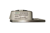
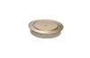
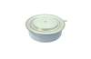
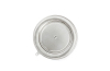
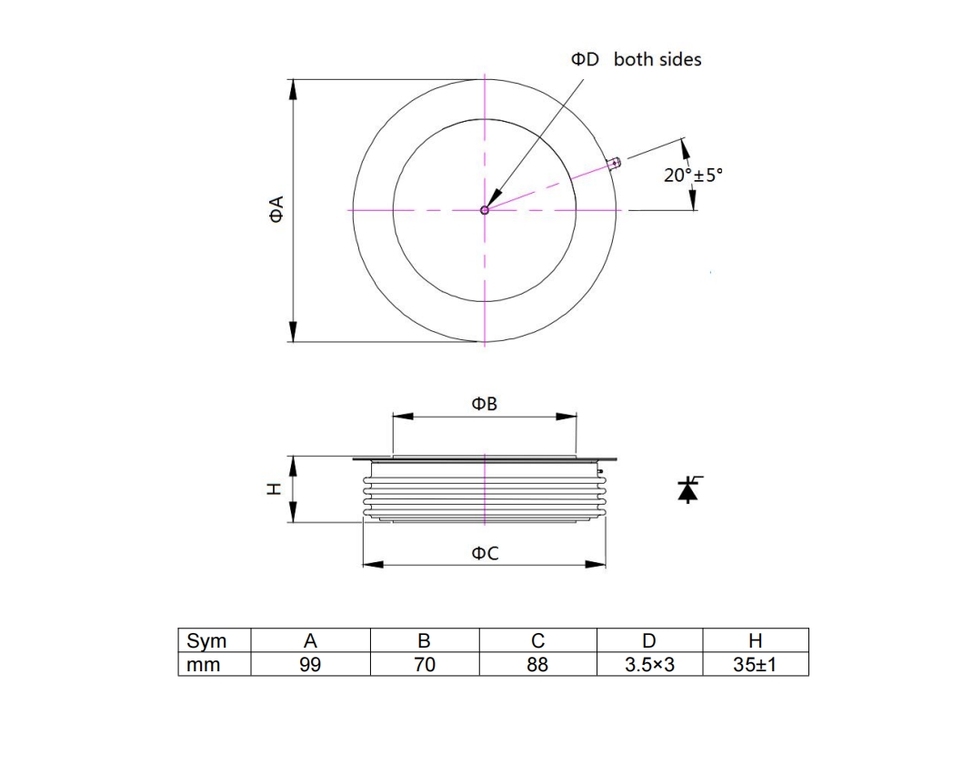
CASE OUTLINE AND DIMENSIONS.

Связанные продукты